- 您现在的位置:买卖IC网 > Sheet目录1905 > ATMEGA8HVA-4CKU (Atmel)MCU AVR 8K FLASH 4MHZ 36-LGA
13
8024A–AVR–04/08
ATmega8HVA/16HVA
7.6
Instruction Execution Timing
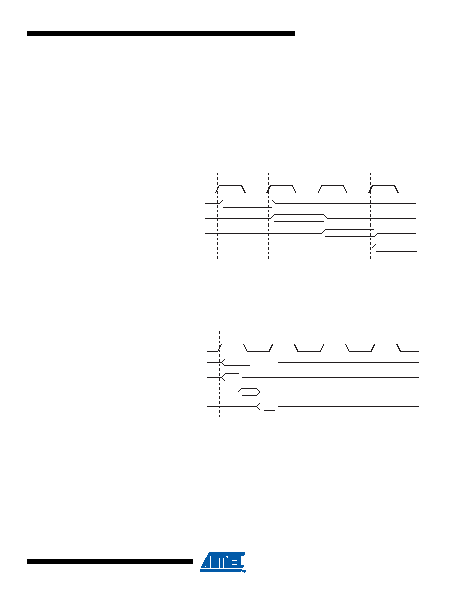
This section describes the general access timing concepts for instruction execution. The AVR
CPU is driven by the CPU clock clk
CPU, directly generated from the selected clock source for the
chip. No internal clock division is used.
Figure 7-4 shows the parallel instruction fetches and instruction executions enabled by the Har-
vard architecture and the fast-access Register File concept. This is the basic pipelining concept
to obtain up to 1 MIPS per MHz with the corresponding unique results for functions per cost,
functions per clocks, and functions per power-unit.
Figure 7-4.
The Parallel Instruction Fetches and Instruction Executions
Figure 7-5 shows the internal timing concept for the Register File. In a single clock cycle an ALU
operation using two register operands is executed, and the result is stored back to the destina-
tion register.
Figure 7-5.
Single Cycle ALU Operation
7.7
Reset and Interrupt Handling
The AVR provides several different interrupt sources. These interrupts and the separate Reset
Vector each have a separate program vector in the program memory space. All interrupts are
assigned individual enable bits which must be written logic one together with the Global Interrupt
Enable bit in the Status Register in order to enable the interrupt.
The lowest addresses in the program memory space are by default defined as the Reset and
Interrupt Vectors. The complete list of vectors is shown in ”Interrupts” on page 52. The list also
determines the priority levels of the different interrupts. The lower the address the higher is the
priority level. RESET has the highest priority.
clk
1st Instruction Fetch
1st Instruction Execute
2nd Instruction Fetch
2nd Instruction Execute
3rd Instruction Fetch
3rd Instruction Execute
4th Instruction Fetch
T1
T2
T3
T4
CPU
Total Execution Time
Register Operands Fetch
ALU Operation Execute
Result Write Back
T1
T2
T3
T4
clk
CPU
发布紧急采购,3分钟左右您将得到回复。
相关PDF资料
ATSAM3N4AA-AU
MCU FLASH 48-QFP
ATSAM3SD8CA-CU
IC MCU 2X256KB CORTEX-M3 100-QFN
ATSAM3U1EB-CU
IC MCU 64KB CORTEX-M3 144-TFBGA
ATSAM3X8EA-CU
IC MCU 2X256KB CORTEX-M3 144-BGA
ATTINY12V-1SUR
IC AVR MCU 1K FLASH 4MHZ 8-SOIC
ATTINY13-20SQR
IC MCU AVR 1KB FLASH 20MHZ 8SOIC
ATTINY13A-MMUR
MCU AVR 1KB FLASH 20MHZ 10DFN
ATTINY13V-10SUR
MCU AVR 1KB FLASH 10MHZ 8SOIC
相关代理商/技术参数
ATMEGA8HVA-4CKUR
功能描述:8位微控制器 -MCU AVR 8KB FLSH 512B EE 1KB SRAM - 4 MHZ RoHS:否 制造商:Silicon Labs 核心:8051 处理器系列:C8051F39x 数据总线宽度:8 bit 最大时钟频率:50 MHz 程序存储器大小:16 KB 数据 RAM 大小:1 KB 片上 ADC:Yes 工作电源电压:1.8 V to 3.6 V 工作温度范围:- 40 C to + 105 C 封装 / 箱体:QFN-20 安装风格:SMD/SMT
ATMEGA8HVA-4TU
功能描述:8位微控制器 -MCU AVR 8KB, 512B EE 4MHz 1KB SRAM 1.8-9V RoHS:否 制造商:Silicon Labs 核心:8051 处理器系列:C8051F39x 数据总线宽度:8 bit 最大时钟频率:50 MHz 程序存储器大小:16 KB 数据 RAM 大小:1 KB 片上 ADC:Yes 工作电源电压:1.8 V to 3.6 V 工作温度范围:- 40 C to + 105 C 封装 / 箱体:QFN-20 安装风格:SMD/SMT
ATMEGA8HVA-4TUR
功能描述:8位微控制器 -MCU AVR 8KB FLSH 512B EE 1KB SRAM - 4 MHZ RoHS:否 制造商:Silicon Labs 核心:8051 处理器系列:C8051F39x 数据总线宽度:8 bit 最大时钟频率:50 MHz 程序存储器大小:16 KB 数据 RAM 大小:1 KB 片上 ADC:Yes 工作电源电压:1.8 V to 3.6 V 工作温度范围:- 40 C to + 105 C 封装 / 箱体:QFN-20 安装风格:SMD/SMT
ATMEGA8HVD-4MX
功能描述:8位微控制器 -MCU AVR 8KB, 512B EE 4MHz 1KB SRAM 2.1-8V
RoHS:否 制造商:Silicon Labs 核心:8051 处理器系列:C8051F39x 数据总线宽度:8 bit 最大时钟频率:50 MHz 程序存储器大小:16 KB 数据 RAM 大小:1 KB 片上 ADC:Yes 工作电源电压:1.8 V to 3.6 V 工作温度范围:- 40 C to + 105 C 封装 / 箱体:QFN-20 安装风格:SMD/SMT
ATMEGA8L-8AC
功能描述:8位微控制器 -MCU AVR 8K FLASH 512B EE 1K SRAM ADC 3V RoHS:否 制造商:Silicon Labs 核心:8051 处理器系列:C8051F39x 数据总线宽度:8 bit 最大时钟频率:50 MHz 程序存储器大小:16 KB 数据 RAM 大小:1 KB 片上 ADC:Yes 工作电源电压:1.8 V to 3.6 V 工作温度范围:- 40 C to + 105 C 封装 / 箱体:QFN-20 安装风格:SMD/SMT
ATMEGA8L8AI
制造商:Atmel Corporation 功能描述:
ATMEGA8L-8AI
功能描述:8位微控制器 -MCU AVR 8K FLASH 512B EE 1K SRAM ADC 3V RoHS:否 制造商:Silicon Labs 核心:8051 处理器系列:C8051F39x 数据总线宽度:8 bit 最大时钟频率:50 MHz 程序存储器大小:16 KB 数据 RAM 大小:1 KB 片上 ADC:Yes 工作电源电压:1.8 V to 3.6 V 工作温度范围:- 40 C to + 105 C 封装 / 箱体:QFN-20 安装风格:SMD/SMT
ATMEGA8L-8AJ
功能描述:IC MCU AVR 8K 5V 8MHZ 32-TQFP RoHS:是 类别:集成电路 (IC) >> 嵌入式 - 微控制器, 系列:AVR® ATmega 标准包装:9 系列:87C 核心处理器:8051 芯体尺寸:8-位 速度:40/20MHz 连通性:UART/USART 外围设备:POR,WDT 输入/输出数:32 程序存储器容量:32KB(32K x 8) 程序存储器类型:OTP EEPROM 大小:- RAM 容量:256 x 8 电压 - 电源 (Vcc/Vdd):4.5 V ~ 5.5 V 数据转换器:- 振荡器型:内部 工作温度:0°C ~ 70°C 封装/外壳:40-DIP(0.600",15.24mm) 包装:管件